PWM 電流制御回路 |
PWM Current Regulator |
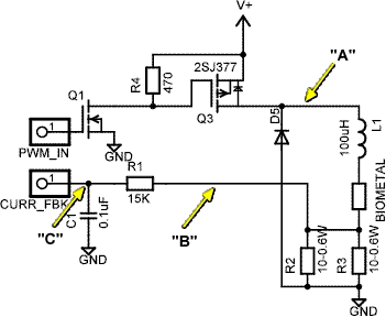
Stainzの改造で遠隔開放カプラを付ける予定ですが、駆動回路が問題なのです。一番簡単なのは抵抗で落とせばいいんですが、バイオメタルの抵抗はほとんど無視できる位、電源電圧として12Vを考えているので抵抗消費分は350mA*12Vで4.2W。 とりあえず、下のようなパワー回路部分を作って、動作確認をして見ます。
|
I am thinking to install a remote-controlled coupler to Stainz. Current driver for the BioMetal is a problem. The simplest way is to provide a resistor to limit the current through BioMetal. I am thinking to use 12VDC for modified Stainz. Tham means the wattage required for the current limiting resistor is about 4.2W (12V X 350mA). It is too much! 10W resistor is required and too large to install in restricted room of the model. Also the heat from the resistor may melt plastic structure. To reduce the heat dissipation from the driver, the driver should be PWM switching mode. So I decided to develop a PWM current driver. Anyway the new contol PCB for Stainz will have a micro controller and it can be used for current control function. I made a power driver on a breadboard to confirm the idea as:
|
||
 |
|||
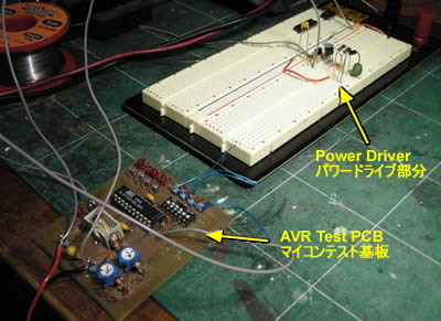 |
This is the test set up. AVR test PCB and power driver on a breadboard are combined. AVR Tiny26のマイコンのテスト用基板とブレッドボードに作ったパワー駆動部分を組み合わせて、テストします。 |
||
|
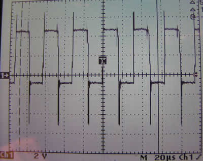
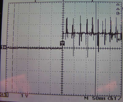
At first the duty of the chopping was fixed to confirm the operation of power circuit. The waveform at “A” was like this. The chopping frequency was about 32KHz. まず、チョッピングのデューティーを固定にして、動作を確認します。”A"部のチョッピング波形はこんな感じ。チョッピング周波数は約32KHzです。 |
||
|
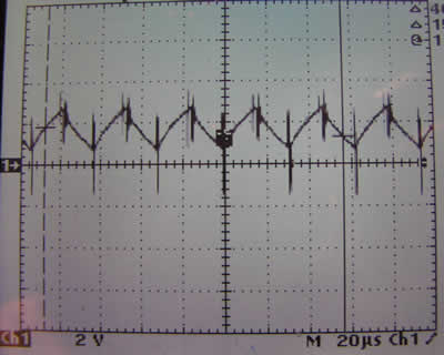
Waveform at “B”, the current, was triangle shape because the movement of the current was retarded by L1. "B"部すなわち電流波形はL1の効果でこのような三角波になります。 |
||
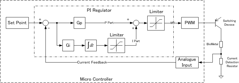
Next enable the current regulation program to actively control the current. I employed PI regulator algorism. Block diagram below shows this algorism. Actual program was coded by Basic and compiled to assembler.
次に電流制御プログラムを活かして、定電流制御にして見ます。 制御アルゴリズムはPI(比例積分)制御としてみました。制御ブロック図は下記のようになります。実際のプログラムはBasicで右のように組みアセンブラに変換しました。
|
Const CC_I_Gain = 10
Const CC_P_Gain = 128 Const CC_Ref = 128 Dim CC_Cont_Flag As Byte If CC_Cont_Flag=1 Then |
||
 |
|||
 |
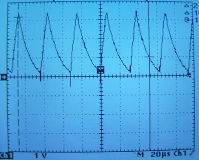
This is the step response of the regulator (at "C"). Response time and stability was acceptable with guessed gains. このPI制御の電流ステップレスポンス("C"部)はこの様になりました。Pゲイン、Iゲインとも適当に設定しましが、応答速度も安定性もまったっく問題ありません。 |
||
 |
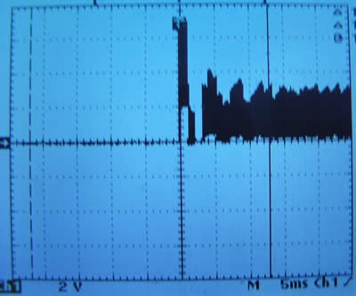
This is the current waveform of product PCB. Above test was done with 5VDC, but actual one is driven from 15VDC. The ripple is much larger than prototype. The gains are retuned. The scan time of the PI regulator is set at 1m sec. これは実際に使う基板での電流波形です。上のテストは5V電源で行いましたが、実際の回路は15Vとなります。このためリップルは5Vの時に比べてはるかに大きくなります。当然、制御常数も変えねばならず、Pゲイン、Iゲインを再調整しました。なお、PI制御演算は1m秒ごとに行う事としました。どうせ、制御対象が抵抗なので、この程度のリップルは全く問題ありません。 |
||
 |
The final step response is like this. On start up it oscillates a bit, but it is not a problem. ステップ応答はこんな感じで、立ち上がりが少しばたばたしますが、問題なし。 |
||